Xiang'an Industrial Park Xiamen Torch High-tech Zone


Industry News
HANDS-ON TEARDOWN | IC-ZD-42 CARRIER TAPE: THE 42MM-WIDE ‘INVISIBLE MOAT’ FOR IC PACKAGE YIELD
Have you ever encountered a situation where the scrap rate suddenly skyrockets during IC placement, pins become inexplicably deformed, or the electrostatic discharge (ESD) failure rate remains stubbornly high? Even though the parameters have been adjusted and the equipment calibrated, the problem keeps recurring, much like ‘Schrödinger’s cat’. Many people’s first instinct is to blame the machinery, but the truth often lies in the most inconspicuous details — the 42mm carrier tape you’re using may simply not be up to the task of high-speed placement for precision ICs.
Today, using the empirically tested IC-ZD-42 carrier tape as an example and in conjunction with the EIA-481 international standard, we’ll break down its dimensions, materials and quality control system to help you avoid 90% of SMT yield pitfalls. I. Why is the 42mm carrier tape considered the “invisible moat” of IC placement?
I. let’s highlight the key points: The IC-ZD-42 is a 42mm-wide, double-row, perforated carrier tape designed specifically for small-sized ICs, addressing three major industry pain points:
High scrap rates during high-speed placement
Prone to pin deformation and scratches
Risk of breakdown in electrostatic-sensitive devices Its value extends far beyond simply ‘mounting components’
— from end-to-end protection from factory to assembly, and from micron-level positioning to ESD protection, every detail determines the final yield rate.
II. Actual Test Data vs International Standards: Just how stringent is the dimensional accuracy of the IC-ZD-42?
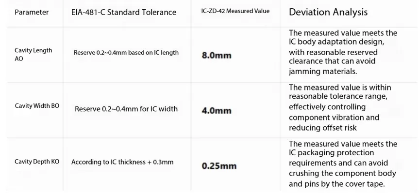
Based on actual test data, we have compared the core cavity dimensions with the EIA-481-C standard. Here is the table with the key findings
III. If the wrong material is chosen, even the strictest dimensional tolerances are of no use. The IC-ZD-42 primarily uses a modified PC (polycarbonate) substrate, whilst ultra-high-speed production lines employ a three-layer composite of ABS and PC. Its core performance directly determines whether it can withstand the rigours of high-speed assembly:
Mechanical Properties: Tensile strength ≥65 MPa; no deformation or cracking during high-speed feeding at 8 m/s
Dimensional Stability: Dimensional drift ≤0.01 mm under temperature variations between -20°C and 60°C
ESD Protection: Modified with carbon powder or conductive particles; surface resistance stabilised at 10⁶–10⁹ Ω, compliant with ESD S20.20 standards
Processing precision: Melting temperature 230–270°C, cavity consistency controlled within ±0.02 mm How to choose for different applications?
Conductive PC (black): 10⁴–10⁶ Ω, suitable for ESD-sensitive components such as high-frequency chips and precision operational amplifiers
Anti-static PC (grey): 10⁷–10¹¹ Ω, suitable for standard small-sized ICs, offering better value for money
ABS/PC composite: Combines toughness and rigidity, suitable for ultra-high-speed placement lines operating at ≥80,000 components per hour.
Warning: Low-temperature embrittlement, ESD attenuation and substrate impurities are three material defects that act as hidden killers, leading to supply issues later on. Pay close attention to these when selecting suppliers.
IV. Comprehensive Inspection System: Stopping Problems Before They Enter the Factory Many factories focus solely on dimensions and neglect the inspection process, resulting in numerous issues once production begins. A complete IC-ZD-42 inspection system must include these 5 steps:
Visual Inspection: Sampling 5% of each batch (no fewer than 5 reels), using a 30x magnifying glass and D65 light source to check for cracks, burrs and impurities
Dimensional Accuracy Inspection: 100% inspection of critical dimensions using a 3D imaging system, with a focus on controlling batch-to-batch variation in A0/B0/K0
ESD Testing: Measure one point at the start, middle and end of each roll; resistance deviation must be ≤1 order of magnitude
Mechanical Performance Testing: Tensile strength ≥65 MPa, peel force 0.2–1.5 N; no adhesive residue or tearing
Environmental Reliability Sampling: Select one roll per batch for high/low temperature and humidity/heat testing to ensure performance stability
V. Common Misconceptions Q&A: Avoid 80% of Pitfalls
Q1: What is the difference between IC-ZD-42 and standard 42mm carrier tape?
A: The key differences lie in dimensional accuracy and ESD stability. The IC-ZD-42 has a cavity tolerance of ±0.03 mm, with measured dimensions of A0=8.00 mm, B0=4.00 mm and K0=0.25 mm, and consistent ESD performance; Standard 42mm carrier tapes have a tolerance of ±0.1mm, with inconsistent ESD performance; mixing them can easily lead to pin deformation and ESD-related scrap.
Q2: Is a high IC placement rejection rate always down to the machine?
A: In 85% of cases, the root cause is carrier tape dimensional deviation! If B0 is too large (>4.20mm), components wobble excessively → rejection; If B0 is too small (<3.80mm), the pins are squeezed → deformation. Rather than repeatedly adjusting the machine, it is better to first check the consistency of the carrier tape’s A0/B0/K0 dimensions.
Q3: What should be prioritised when selecting a supplier?
A: Prioritise manufacturers with EIA-481 compliance + ISO9001 certification, equipped with in-line 3D imaging inspection. Focus on three key points: dimensional consistency, long-term ESD stability, and mass delivery capability.
Q4: How should carrier tapes be stored to prevent failure later on?
A: Store in a sealed container at 20–25°C and 40–60% RH, with a storage period not exceeding six months; once opened, use within 24 hours where possible; maintain a humidity level of ≥35% in the assembly workshop to minimise static build-up. Final Thoughts: Improving SMT yield has never been about applying ‘patches’ after the fact, but rather about preventing errors at the source. A small 42mm carrier tape embodies a holistic control logic spanning standards, materials and inspection. What carrier tape-related pitfalls have you encountered on the production line? Let’s discuss in the comments section!
Diam luctus nostra dapibus varius et semper semper
rutrum ad risus
eros. Cursus libero viverra tempus netus diam vestibulum

GET FREE QUOTE
Please contact us.